
Provide the accumulated technical know-how
On the logic design in front-end design, We are response to various needs based on our experience and accumulated technical capabilities in many fields such as image processing and optical disk etc. In addition, we have techniques in back-end design such as P&R and timing-closure etc. Also, in the circuit design, we are introducing the system level design languages such as SystemC for the co-design of the software, in addition to hardware description language Verilog-HDL or VHDL.
SANEI HYTECHS VIETNAM focus the logic design and functional verification in front-end design, and FPGA design service.
FPGA Design service
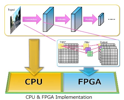
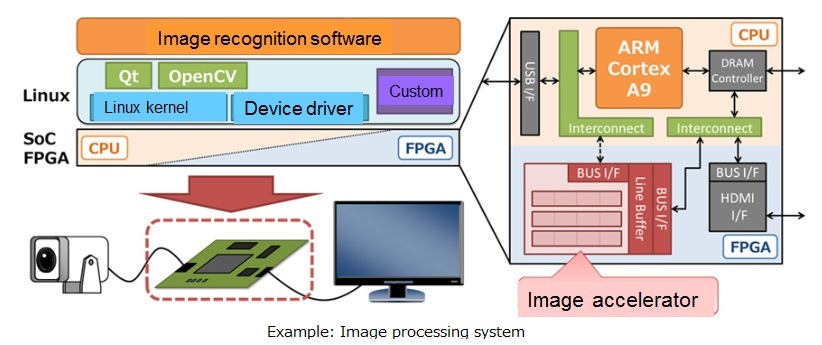
The demand of FPGA which can be implemented the required functions at low cost and short-term design period has been increasing. In design with using FPGA, it also have great benefit that we can check operation test immediately after circuit design or specification changes. In addition, the demand for FPGA design with a built-in high-performance processor such ARM has been increasing. Taking advantage of accumulated LSI design technology, we offer FPGA design services. We correspond a wide range customer’s request from specification study to the actual operation evaluation. Sanei Hytechs is the Certified Partner of Xilinx Alliance Program (XAP).
Also, Sanei Hytechs is working on the implementation of Artificial Intelligence (AI) on FPGA including CPU.
LSI Design service
- Functional/Logic Design
Based on the determined specification, we decide the functional structure of LSI. First, we clarify the role of Hardware and Software in the functional configuration. Then, we consider the algorithm and pipelining , do the logic design of outline.
- Functional RTL Design
By using a hardware description language such as Verilog-HDL or VHDL, we describe the LSI function. We also use the latest description languages such as SystemC.
- Functional Verification
Using the logic simulator, we verify whether the RTL stated operates correctly based on functional specification. We also use Assertion-based verification.
- Logic Synthesis
After functional verification, We convert RTL description to the gate level netlist. Also, we optimize circuit so as to satisfy the constraints such as area and speed.
- Gate-Level Verification
We verify the operation of the circuit of the gate level by the logic simulator with using the test pattern. We set wiring load capacitance in the virtual conditions.
- Physical Layout Design (P&R)
According to the actual circuit diagram, we design transistors and wiring by using an automatic placement and routing tool.
- Timing Verification
By using a static timing analysis tool, we check all of the path which has possibility of a timing violation, and validate the timing performance of the design.
- Layout Verification
We verify whether the layout pattern meets the design rules. After all has been cleared, the sample chip is created.